
Following the mass deployment of Blackwell GB200 systems, NVIDIA has officially detailed the silicon roadmap for its next-generation computational platform: the Rubin R100 GPU. Manufactured on TSMC's 3nm Gate-All-Around (GAA) nanosheet process and packaging 288GB of high-speed HBM4 memory, Rubin addresses the primary bottleneck throttling frontier frontier models—memory bandwidth limits in the Key-Value (KV) cache during autoregressive generation.
Featuring a 2048-bit wide HBM4 memory bus delivering over 10.5 TB/s of sustained memory bandwidth per GPU and NVLink 6 interconnects running at 3.6 TB/s, the Rubin architecture allows multi-trillion parameter Mixture-of-Experts (MoE) models to serve live inference without stalling compute engines.
The Memory Wall: Why HBM4 Changes the Packaging Blueprint
For the past three GPU generations (A100, H100, B200), High Bandwidth Memory relied on a standardized 1024-bit interface per stack. To expand bandwidth, engineers were forced to increase data transfer clock rates on the silicon interposer, leading to severe thermal throttling, dielectric degradation, and signal integrity drops.
HBM4 shatters this architectural constraint by doubling the physical bus width to 2048 bits per memory stack. Because the interface is twice as wide, the memory achieves vastly higher total throughput while operating at cooler, power-efficient clock frequencies:
- Direct Logic-Base Die Integration: Unlike HBM3e where the base die was a passive silicon interposer, HBM4 base dies are manufactured directly on TSMC 3nm/5nm logic nodes, allowing built-in memory scheduling and direct BIST (built-in self-test) diagnostics.
- 288GB VRAM Capacity per Package: Utilizing 16-high (16-Hi) DRAM die stacks with hybrid bonding (direct copper-to-copper micro-bumps), Rubin integrates 8 HBM4 stacks around the dual-reticle logic dies, unlocking 288GB of unified VRAM.
- 10.5 TB/s Memory Bandwidth: Compared to Blackwell's 8.0 TB/s (HBM3e), Rubin achieves a 31% increase in raw memory throughput, resolving execution bubbles during large batch size inference.
| Metric / Architecture | NVIDIA Hopper H100 | NVIDIA Blackwell B200 | NVIDIA Rubin R100 |
|---|---|---|---|
| Fabrication Process | TSMC 4N (5nm FinFET) | TSMC 4NP (Custom 5nm) | TSMC 3nm GAA Nanosheet |
| Die Architecture | Monolithic (814 mm²) | Dual-Die CoWoS-L (2x Reticle) | Quad-Chiplet System-on-Package |
| Memory Subsystem | 80GB HBM3 (1024-bit) | 192GB HBM3e (1024-bit) | 288GB HBM4 (2048-bit) |
| Memory Bandwidth | 3.35 TB/s | 8.0 TB/s | 10.5+ TB/s |
| Interconnect Fabric | NVLink 4 (900 GB/s) | NVLink 5 (1,800 GB/s) | NVLink 6 (3,600 GB/s) |
| Native Precision Modes | FP8, FP16, BF16 | FP4, FP8, FP16 | Micro-Scaling FP4, FP2 Experimental |
NVLink 6: 3.6 TB/s Bi-Directional Fabric for Trillion-Parameter MoE
In modern Mixture-of-Experts architectures like DeepSeek V3 and OpenAI o3, token routing requires sending token embeddings to disparate GPUs across the rack within microseconds. When the interconnect saturates, GPU tensor cores sit idle waiting for all-to-all communication collectives.
Rubin introduces NVLink 6, which doubles bi-directional bandwidth to 3.6 TB/s per GPU. Implemented through 224 Gbps PAM4 optical and copper transceivers, NVLink 6 allows a full 72-GPU liquid-cooled rack (Rubin NVL72) to function as a singular coherent computing node with 20.7 terabytes of aggregate ultra-high-speed memory and 259 TB/s of bisection bandwidth.
Micro-Scaling Formats: Pushing Inference into FP4
Rubin expands second-generation Transformer Engines with native support for micro-scaled FP4 (Micro-Scaling Tensor Cores). Rather than applying a single scaling factor across an entire matrix, micro-scaling applies independent scaling factors across microscopic blocks of 16 elements.
This architectural enhancement preserves mathematical convergence during reasoning generation while slashing the memory footprint by 75% compared to 16-bit floats. Consequently, enterprise clusters can host active reasoning context windows exceeding one million tokens on a fraction of the hardware footprint previously demanded by Hopper clusters.
Thermal Density & Direct-to-Chip Liquid Cooling Realities
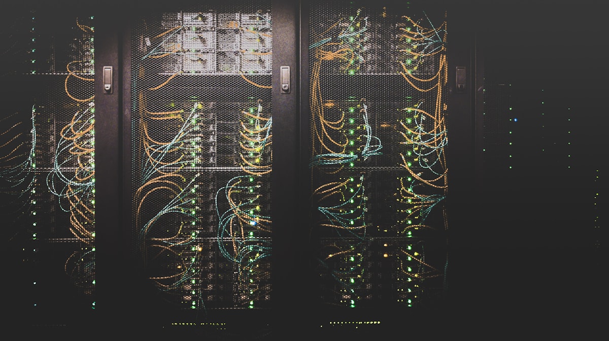
With thermal design power (TDP) per Rubin GPU reaching upwards of 1,200W to 1,400W in dense compute configurations, air cooling is completely obsolete. Datacenters adopting Rubin architectures require 100% direct-to-chip liquid cooling setups using facility water temperatures up to 45°C.
By coupling TSMC's 3nm nanosheets with 288GB HBM4 and NVLink 6 fabrics, NVIDIA establishes a high-performance computational baseline designed to power the next decade of frontier artificial intelligence.

💬 Reader Discussion & Feedback 0